TSMC is replacing its workhorse CoWoS packaging with a panel-level technology called CoPoS that uses rectangular glass substrates instead of circular silicon wafers, boosting material utilization above 90% from below 70% and cutting costs by 20% to 30% per unit area, according to supply chain sources and Taiwanese media reports.
"CoPoS adopts a panel-level packaging that transforms the circle into a square, which can significantly increase the material utilization rate of the original 12-inch circular wafer from less than 70% to more than 90%, solving the problem of geometric waste and soaring costs caused by the maximization of photomask size in ultra-large AI chips after 2028," the Commercial Times reported, citing industry sources.
The first wave of demo equipment has been delivered to TSMC subsidiary VisEra's Longtan plant in Taiwan, with nearly 30 vendors from Japan, the US, Germany and Taiwan making the initial evaluation list. The equipment spans six process areas: exposure and coating, metallization and copper plating, grinding and laser processing, wet processing and heat treatment, molding and reflow, and measurement and inspection. Key suppliers include Canon for exposure tools, Applied Materials and Lam Research for metallization, DISCO for grinding, and KLA for inspection — though most remain in the demo phase, with formal purchase orders typically requiring about 18 months of validation.
TSMC Chairman C.C. Wei first disclosed CoPoS during the company's April 2026 earnings call, and the company has since applied for the "TSMC-COPOS" trademark with Taiwan's Intellectual Property Office. The technology targets AI GPU and high-performance computing chips that require increasingly large packaging footprints — future GPUs may need a packaging solution far exceeding what CoWoS's 300mm wafer can economically deliver. CoPoS panels can scale to 750 by 620mm, compared with CoWoS's 300mm circular wafer, enabling larger compute dies and higher volumes per panel.
Glass Substrate Brings Tradeoffs
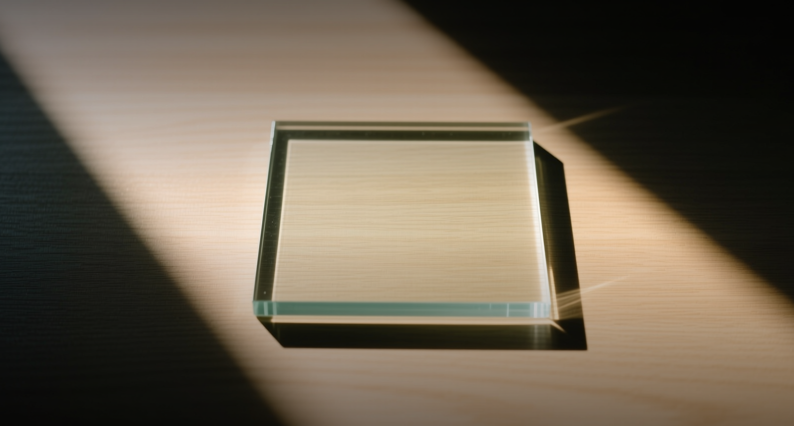
The shift to glass core substrates is central to CoPoS's performance gains but introduces manufacturing challenges. Through-glass vias improve the warpage index by 16% compared with organic substrates and reduce electrical inductance and resistance, enabling larger packages with more dies. Glass, however, is brittle — a microscopic scratch can evolve into structural damage under stress — and its electrical conductivity is inferior to silicon, creating hurdles for high-power applications.
TSMC's initial panel size target is 310 by 310mm, with pilot production slated for 2027 and mass production in the second half of 2028. Full adoption of glass core substrates is not expected until after 2030. The company is working with Ibiden and Innolux to develop a three-layer glass core design with the glass sandwiched between two ABF layers. Production may extend to VisEra's Chiayi site in Taiwan or to TSMC's Arizona fab between 2029 and 2030.
Taiwanese equipment makers are positioning for the transition. Manz Automation is preparing tools for TGV metallization and RDL processing. InnoService expects its copper column deposition machines ready for mass production by 2027. Scientech and Grand Process Technology are providing wet processing and cleaning tools, while Chroma is developing panel inspection systems. V5 Tech, Favite, and Weike Semi are among the Taiwanese firms supplying measurement and inspection equipment for glass substrates — a segment that previously offered limited entry points in the CoWoS supply chain.
Competitive Stakes and Investor Impact
Intel is pursuing a parallel glass substrate strategy at its Rio Rancho facility in New Mexico, which the company has described as the "crown jewel" for advanced packaging. Amkor has stated that Intel's glass substrate technology will be ready for commercialization within three years. The race to panel-level packaging means both foundries are investing heavily in new equipment ecosystems, with TSMC's roughly 30-vendor list signaling the scale of capital required.
AMD is expected to be a key customer for TSMC's fan-out panel-level packaging and 1.4nm process for its client-focused Zen 7 lineup, expected in 2028. The adoption of CoPoS extends beyond client applications into AI and data center markets, where packaging capacity has become a bottleneck for GPU supply. TSMC's CoWoS capacity has been sold out for consecutive quarters, and CoPoS represents the company's answer to a packaging demand that CoWoS alone cannot satisfy.
For investors, the CoPoS ramp creates both opportunity and risk. Equipment makers named to the initial vendor list — including Applied Materials, Lam Research, Canon, DISCO, and KLA — could see sustained demand as TSMC builds out panel-level production lines. Taiwanese suppliers such as Scientech, Grand Process Technology, and Chroma gain exposure to a new revenue stream that did not exist in the CoWoS era. But the 18-month validation cycle means near-term revenue from CoPoS equipment orders remains limited, and not all demo-stage vendors will convert to production contracts. TSMC itself trades at roughly 22 times forward earnings, with the CoPoS investment cycle already reflected in elevated 2026 capital expenditure guidance of $38 billion to $42 billion.
This article is for informational purposes only and does not constitute investment advice.