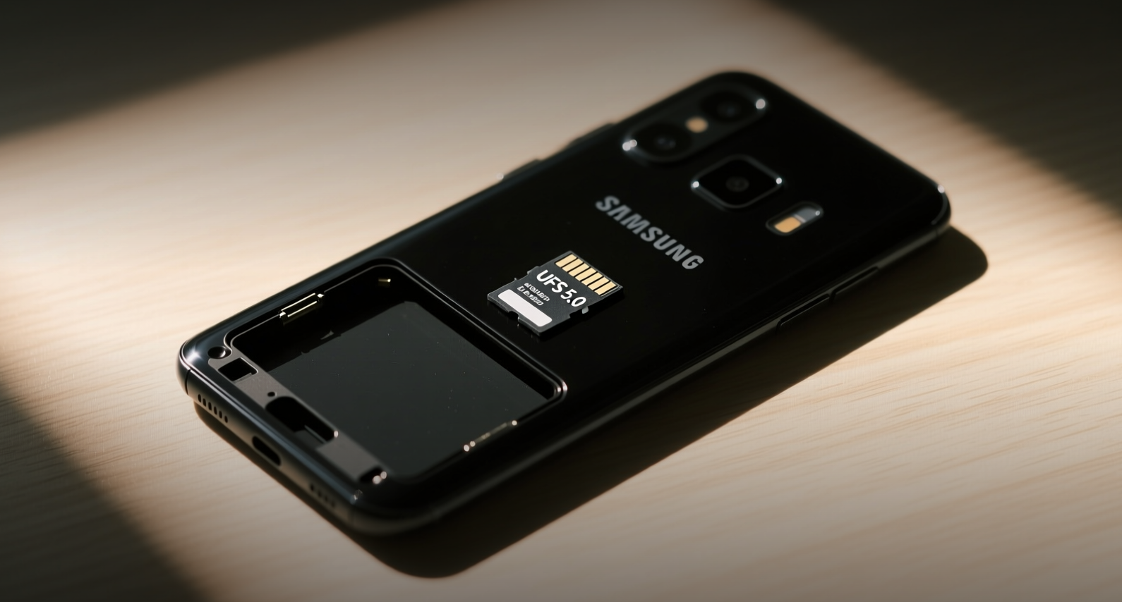
Samsung's new UFS 5.0 memory reads data at 10.8 GB/s, more than double the prior generation, targeting the surge in on-device AI processing.
Samsung Electronics developed the industry's fastest UFS 5.0 storage solution with 10.8 GB/s sequential read speeds, more than doubling the performance of its predecessor to handle large language models on mobile devices.
"In the era of on-device AI, storage devices are evolving into a key driver defining AI experiences," Jangseok Choi, head of Memory Product Planning at Samsung Electronics, said.
The UFS 5.0 delivers sequential write speeds of 9.5 GB/s, more than twice the UFS 4.1 standard. Power efficiency improved by more than 40% through clock gating and multi-voltage technologies. The package measures 7.5mm by 13mm by 0.9mm, 16.7% smaller than its predecessor, boosting design flexibility for mobile, wearable and extended reality devices.
Mass production begins in the fourth quarter of 2026 with capacities up to 1 TB. The technology targets flagship smartphones, XR headsets and AI wearables — markets where on-device AI processing demands faster local storage to run large language models without cloud latency.
How UFS 5.0 Changes the On-Device AI Calculus
Generative AI is shifting from cloud-based inference to local processing, driving a surge in data that must be stored and retrieved on the device itself. Storage is evolving from a medium used primarily to hold files to core infrastructure that supports AI computation. Samsung's UFS 5.0 integrates the latest JEDEC embedded memory interface standard to achieve the industry's highest bandwidth of 10.8 GB/s.
The speed gain matters because large language models require rapid access to model weights and parameters stored in local memory. A smartphone running a 7-billion-parameter model locally needs to load hundreds of megabytes of data in milliseconds. UFS 5.0's 10.8 GB/s throughput cuts that loading time roughly in half compared with UFS 4.1, reducing the delay between a user query and the model's response.
Competitive Pressure on Rivals
Samsung's announcement puts pressure on SK Hynix and Micron Technology, both developing their own high-speed mobile memory solutions. SK Hynix has focused on HBM for AI accelerators, while Micron has pushed its 232-layer NAND for mobile applications. Samsung's UFS 5.0 leap gives it a potential first-mover advantage in the premium smartphone storage segment, where Apple and Qualcomm-powered Android flagships compete for AI performance leadership.
Samsung manufactures its own NAND flash and controllers internally, giving it vertical integration advantages over competitors that rely on third-party controller designs. The company plans to scale up supply to meet demand from next-gen device markets, ranging from flagship smartphones to XR headsets and AI wearables.
Investor Impact
Samsung Electronics (KRX: 005930) trades at about 1.2 times book value, reflecting the conglomerate's mature memory business. The UFS 5.0 breakthrough could support margin expansion in the memory segment, which generated about 30 trillion won in operating profit in 2025. For investors, the key question is whether Samsung can convert its technology lead into pricing power before competitors match the specification. SK Hynix (KRX: 000660) and Micron (MU:US) face pressure to accelerate their own roadmaps or risk losing share in the premium mobile storage market.
This article is for informational purposes only and does not constitute investment advice.