Key Takeaways:
- Qnity launched an Advanced Packaging Innovation Hub on June 22, 2026
- The hub targets the industry shift from transistor shrink to 3D chip stacking
- Qnity provides materials across the full packaging stack for AI chip demand
Key Takeaways:
The semiconductor industry's next battleground is no longer how small you can etch a transistor, but how many chips you can stack on top of each other.
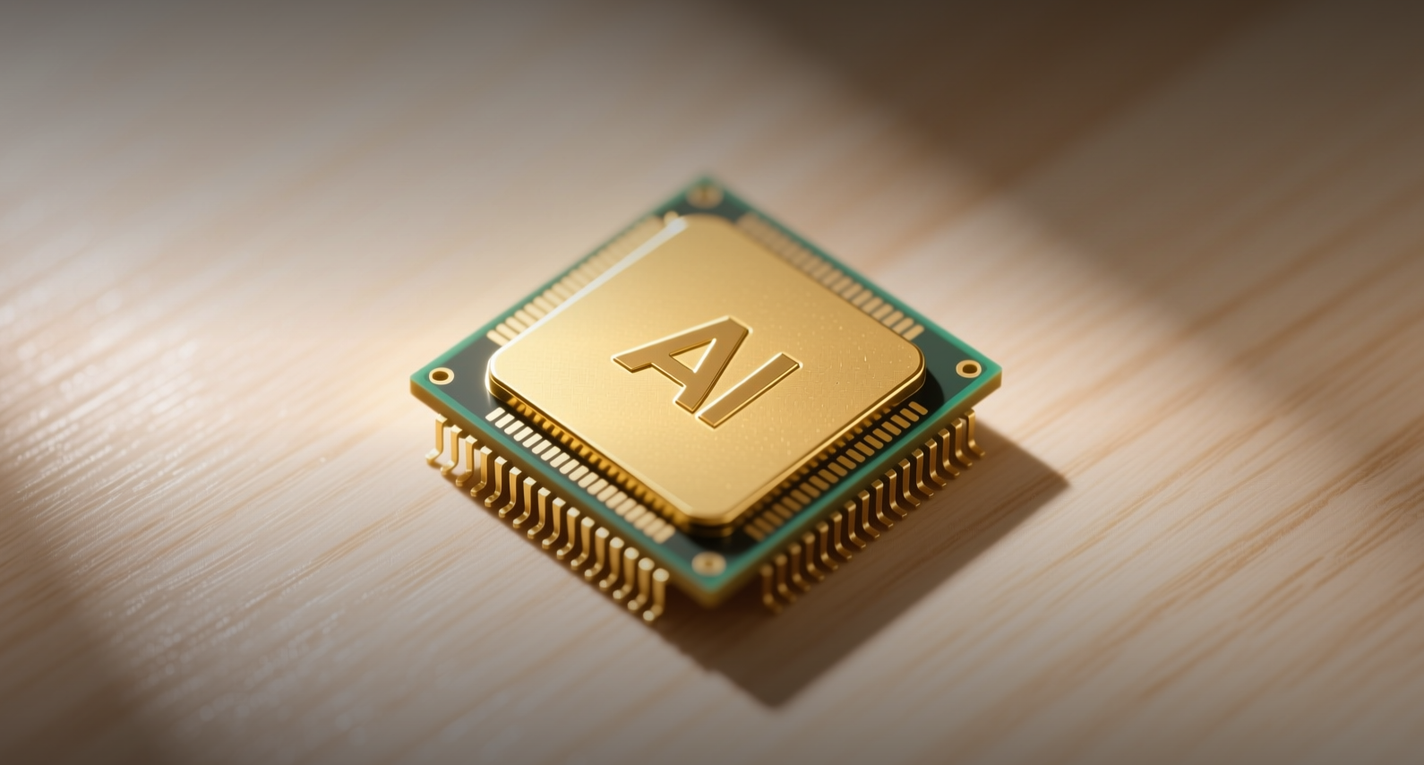
Qnity Electronics Inc. (NYSE: Q) launched its Advanced Packaging Innovation Hub on Monday, betting that the shift from shrinking transistors to stacking chips in 3D architectures will become the semiconductor industry's primary growth engine for AI infrastructure. The online platform showcases the company's materials and process technologies across the full advanced packaging stack, from high-bandwidth memory (HBM) and interposers to hybrid bonding and IC substrates.
"As AI reshapes computing, the hardest engineering problems are moving into the connections between chips, layer to layer — where performance, power, density, and reliability are decided," Chuck Xu, President of Interconnect Solutions at Qnity, said. "That's where Qnity shines. We bring our semiconductor and interconnect strengths together so customers can master advanced packaging from design through system integration, end-to-end."
Advanced packaging refers to techniques that arrange and connect multiple chips in tight 3D stacks rather than placing them separately on a circuit board. The approach has become essential as traditional transistor scaling — the "shrink" driven by Moore's Law — delivers diminishing returns. Chipmakers now rely on methods such as through-silicon vias (TSVs), which are tiny vertical connections drilled through silicon to link stacked layers, and hybrid bonding, which joins chips face-to-face using microscopic metal and insulating connections. Qnity's solutions target precisely these manufacturing challenges, including defect reduction, thermal management, and high-density routing for multi-die designs.
The announcement positions Qnity to capture demand from the AI chip ecosystem, where Nvidia, AMD, and a growing roster of custom silicon designers require increasingly complex packaging to connect compute dies with HBM memory stacks. Advanced packaging has emerged as a bottleneck in AI chip production, with TSMC's CoWoS (chip-on-wafer-on-substrate) capacity consistently oversubscribed through 2025 and into 2026. Qnity, as a materials and interconnect provider, sits upstream of the foundries and outsourced semiconductor assembly and test (OSAT) providers such as ASE Technology and Amkor Technology that perform the actual packaging.
The company's portfolio spans the materials needed for each layer of the packaging stack: metallization chemicals for fine-line redistribution layers (RDLs), dielectric materials for interposers, and bonding technologies for multi-die integration. These inputs are critical for achieving the yield and reliability required as chip designs grow more complex — some AI accelerators now integrate more than a dozen chiplets in a single package.
For investors, Qnity's strategic emphasis on advanced packaging signals a deliberate pivot toward the fastest-growing segment of the semiconductor materials market. The company trades on the New York Stock Exchange under the ticker Q, and its interconnect solutions business has been a steady revenue contributor as AI infrastructure buildouts drive demand for high-speed data transmission within and between chips. The launch of the Innovation Hub provides a centralized showcase for customers evaluating packaging materials, potentially shortening design cycles and accelerating qualification timelines.
The shift from shrink to stack is reshaping the competitive landscape across the semiconductor value chain. Equipment makers such as Applied Materials and ASML have long dominated the transistor-shrink era; the packaging transition opens new opportunities for materials specialists like Qnity, as well as for OSAT providers and design software firms. Chipmakers that master advanced packaging gain performance advantages without requiring the next-generation lithography node — a particularly valuable capability as 2nm and below become exponentially more expensive to develop.
This article is for informational purposes only and does not constitute investment advice.